|

MOSFET Used In Battery Charger
Product Details:
- Product Type SJ-FET
1.00 - 10.00 USD ($)/Piece
X
MOSFET Used In Battery Charger Price And Quantity
- 1.00 - 10.00 USD ($)/Piece
- 10000 Piece
MOSFET Used In Battery Charger Product Specifications
- SJ-FET
MOSFET Used In Battery Charger Trade Information
- 20000 Piece Per Month
- 7-15 Days
- Asia Australia Central America North America South America Eastern Europe Western Europe Middle East Africa
Product Description
All series of our products (good price performance) are confirmed and popular with the worldwide users, our products have been exported far to Europe, North & sounth America,Japan,south Korea,south-east area and Mid-east area etc.Welcomed you to customer-made and do OEM for current products and new products,and we are looking forward to set up one long-term cooperation relations with you too. Please feel free to contact us for further information.
Packaging and Internal Circuit :
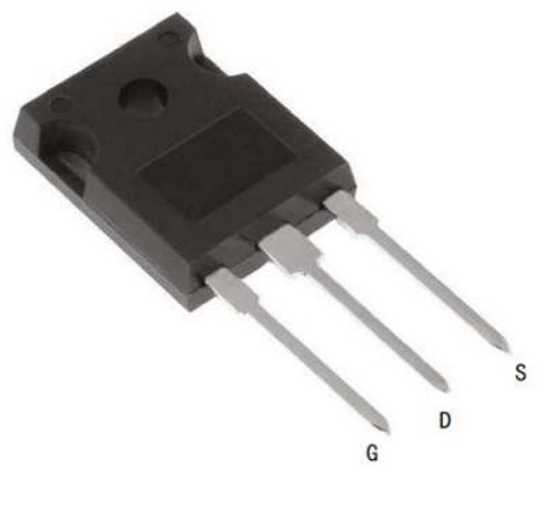
| Part Name | Package | Marking |
| RTW65R041E | TO247 | RTW65R041E |
Key Performance Parameters :
| Parameter | Value | Unit |
| VDS @ Tj,max | 700 | V |
| RDS(on),max | 41 | m |
| Qg,typ | 133.5 | nC |
| ID,pulse | 240 | A |
Maximum ratings :
| Parameter | Symbol | Values | Unit | Note / Test Condition | ||
| Min. | Typ. | Max. | ||||
| Continuous drain current1) | /D | | - | 80 | A | TC=25C |
| Pulsed drain current2) | ID, pulse | - | - | 240 | A | TC=25C |
| Avalanche energy, single pulse | EAS | - | - | 980 | mJ | Tc=25oC, VDD=50V, L=10mH, RG=25 |
| MOSFET dv/dt ruggedness | dv/dt | - | - | 4.7 | V/ns | VDS=0...150V |
| Gate source voltage (static) | VGS | -20 | - | 20 | V | static; |
| Gate source voltage (dynamic) | VGS | -30 | - | 30 | V | AC (f>1 Hz) |
| Power dissipation | Ptot | - | - | 481 | W | TC=25C |
| Storage temperature | Tstg | -55 | - | 150 | C | |
| Operating junction temperature | Tj | -55 | - | 150 | C | |
| Reverse diode dv/dt3) | dv/dt | - | - | 15 | V/ns | VDS=0...400V, ISD<=IS, Tj=25C |
Thermal characteristics :
| Parameter | Symbol | Values | Unit | Note / Test Condition | ||
| Min. | Typ. | Max. | ||||
| Thermal resistance, junction - case | RthJC | - | - | 0.26 C/W | - | |
| Thermal resistance, junction - ambient | RthJA | - | - | 62 C/W | | device on PCB, minimal footprint |
Static characteristics :
| Parameter | Symbol | Values | Unit | Note / Test Condition | ||
| | Min. | Typ. | Max. | |||
| Drain-source breakdown voltage | V(BR)DSS | 655 | - | - | V | VGS=0V, ID=10mA |
| Gate threshold voltage | V(GS)th | - | | 4.2 | V | VDS=VGS, ID=250uA |
| Zero gate voltage drain current | IDSS | - | - | 1 | uA | VDS=650V, VGS=0V, Tj=25oC |
| Gate-source leakage current | IGSS | - | - | 100 | uA | VGS=30V, VDS=0V |
| Drain-source on-state resistance | RDS(on) | - | 0.034 | 0.041 | VGS=10V, ID=28A, Tj=25oC | |
| Gate resistance (Intrinsic) | RG | - | 13 | - | f=1MHz, open drain | |
Dynamic characteristics
| Parameter | Symbol | Values | Unit | Note / Test Condition | ||
| Min. | Typ. | Max. | ||||
| Input capacitance | Ciss | - | 5966 | - | pF | VGS=0V, VDS=50V, f=1MHz |
| Output capacitance | Coss | - | 464 | - | pF | VGS=0V, VDS=50V, f=1M Hz |
| Reverse transfer capacitance | Crss | - | 53 | - | pF | VGS=0V, VDS=50V, f=1M Hz |
| Turn-on delay time | td(on) | - | 50.4 | - | ns | VDD=400V,VGS=13V,ID=49.6A RG=1.7;see table 9 |
| Rise time | tr | - | 46.8 | - | ns | VDD=400V,VGS=13V,ID=49.6A RG=1.7;see table 9 |
| Turn-off delay time | td(off) |
| - | 326 | - | ns VDD=400V,VGS=13V,ID=49.6A RG=1.7;see table 9 |
| Fall time | tf | - | 48 | - | ns | VDD=400V,VGS=13V,ID=49.6A RG=1.7;see table 9 |
Gate charge characteristics :
| Parameter | Symbol | Values | Unit | Note / Test Condition | ||
| Min. | Typ. | Max. | ||||
| Gate to source charge | Qgs | - | 38.6 | - | nC | VDD =400V, ID =49.6A, VGS =10V |
| Gate to drain charge | Qgd | - | 60 | - | nC | VDD =400V, ID =49.6A, VGS =10V |
| Gate charge total | Qg | - | 133.5 | - | nC | VDD =400V, ID =49.6A, VGS =10V |
| Gate plateau voltage | Vplateau | - | 7.0 | - | V | VDD =400V, ID =49.6A, VGS =10V |
Reverse diode characteristics :
| Parameter | Symbol | Values | Unit | Note / Test Condition | ||
| Min. | Typ. | Max. | ||||
| Diode forward voltage | VSD | - | 0.65 | - | V | VGS=0V, IF=1A, Tj=25C |
| Reverse recovery time | trr | - | 802 | - | ns | Vr=400V,IF=49.6A,di/dt=100A/us see table 8 |
| Reverse recovery charge | Qrr | - | 23.21 | - | uC | Vr=400V,IF=49.6A,di/dt=100A/us see table 8 |
| Peak reverse recovery current | Irrm | - | 50 | - | A | Vr=400V,IF=49.6A,di/dt=100A/us see table 8 |
Enter Buying Requirement Details
Other Products in 'Mosfet Power Semiconductor' category
We are
accepting inquiries from these countries India, Sri Lanka, Pakistan,
Bangladesh, Afghanistan and Nepal.
RONGTECH INDUSTRY (SHANGHAI) INC.
- Room - 1123-1127, No.81 South QinZhou Road, XuHui,Shanghai - 200235, China
- Phone : 86-21-64516109
- Fax :86-21-54481689
- Mr. Droden Zhang (Sales Manager)
- Mobile : +8618001811078
- Send Inquiry
- Model:0086-18001811078

RONGTECH INDUSTRY (SHANGHAI) INC.
All Rights Reserved.(Terms of Use)
Developed and Managed by Infocom Network Private Limited.
Developed and Managed by Infocom Network Private Limited.
