|

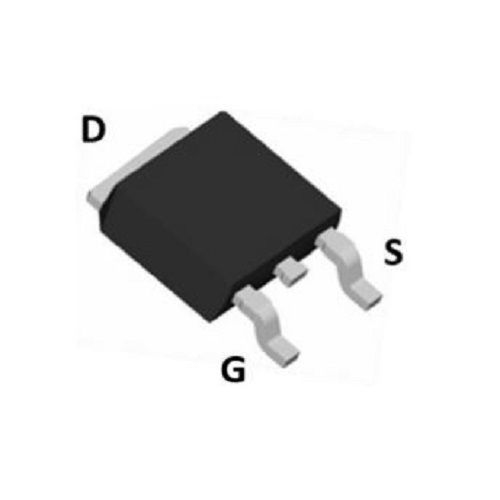
Low Voltage Mosfet
X
Low Voltage Mosfet Price And Quantity
- 1.00 - 10.00 USD ($)/Piece
- 10000 Piece
Low Voltage Mosfet Trade Information
- 20000 Piece Per Month
- 7-15 Days
- Asia Australia Central America North America South America Eastern Europe Western Europe Middle East Africa
Product Description
Description:
The RM series products utilizes Norsem's outstanding standard turbo process and packaging techniques to achieve ultral low on-resistance and low gate charge and to provide the industry's best-in-class performance. These features make this series products extremely efficient, temperature characteristics and reliable for use in power management, synchronous rectification, battery protection, load switch and a wide variety of other applications.
Features and Benefits:
- Standard Turbo MOSFET process technology.
- Optimized the cell structure.
- Low on-resistance and low gate charge.
- Featuring low switching and drive losses.
- Fast switching and reverse body recovery.
- High ruggedness and robustness.
Main Product Characteristics :
| V(BR)DSS | 30V |
| RDS(ON) | 5.8m(max.) |
| ID | 100A |
Absolute Maximum Ratings (TC=25oC unless otherwise specified)
| Parameter | Symbol | Max. | Unit |
| Drain-Source Voltage | VDS | 30 | V |
| Gate-to-Source Voltage | VGS | + 20 | V |
| Continuous Drain Current, @ Steady-State 1 | ID @ TC = 25oC | 100 | A |
| Continuous Drain Current, @ Steady-State | ID @ TC = 100oC | 68 | A |
| Pulsed Drain Current 2 | IDM | 400 | A |
| Power Dissipation | PD @TA = 25oC | 83 | W |
| PD @TA = 100oC | 37.8 | ||
| Linear Derating Factor | TA = 25oC | 0.66 | W/oC |
| Single Pulse Avalanche Energy3 | EAS | 780 | mJ |
| Junction-to-Case | RJC | 0.6 | oC/W |
| Junction-to-Ambient (PCB Mounted, Steady-State) 4 | RJA | 62.5 | oC/W |
| Operating Junction and Storage Temperature Range | TJ /TSTG | -55 to + 150 | oC |
Electrical Characteristics (TC=25oC unless otherwise specified)
| Parameter | Symbol | Conditions | Min. | Typ. | Max. | Unit |
| Drain-to-Source Breakdown Voltage | V(BR)DSS | VGS=0V, ID=250A | 30 | - | - | V |
| Drain-to-Source Leakage Current | IDSS | VDS=30V, VGS=0V | - | - | 1 | uA |
| TJ=125oC | - | - | 50 | |||
| Gate-to-Source Forward Leakage IGSS | IGSS | VGS =20V | - | - | 100 | nA |
| VGS =-20V | - | - | -100 | |||
| Static Drain-to-Source On- Resistance | RDS (on) | VGS=10V, ID=50A | - | 4.3 | 5.8 | m |
| VGS=4.5V, ID=15A | - | 5.2 | 7.5 | |||
| Gate Resistance | Rg | f-1MHz | - | 1.8 | - | |
| Gate Threshold Voltage | VGS (th) | VDS=VGS, ID=250uA | 1.0 | 1.6 | 2.6 | V |
| Input Capacitance | Ciss | VGS=0V, VDS=5V | - | 2180 | - | pF |
| Output Capacitance | Coss | - | 270 | - | ||
| Reverse transfer capacitance | Crss | - | 210 | - | ||
| Total Gate Charge | Qg | ID=30A, VDS=24V, VGS=10V | - | 47.2 | - | nC |
| Gate-to-Source Charge | Qgs | - | 8.8 | - | ||
| Gate-to-Drain("Miller") Charge | Qgd | - | 9.6 | - | ||
| Turn-on Delay Time | td (on) | VGS=4.5V, VDD=20V, ID=60A, RGEN=1.8 | - | 12.3 | - | nS |
| Rise Time | tr | - | 87.3 | - | ||
| Turn-Off Delay Time | td (off) | - | 140 | - | ||
| Fall Time | tf | - | 82.4 | - | ||
| Source-Drain Ratings and Characteristics | ||||||
| Parameter | Symbol | Conditions | Min. | Typ. | Max | Unit |
| Continuous Source Current (Body Diode) | Is | MOSFET symbol showing the integral reverse p-n junction diode. | - | - | 100 | A |
| Pulsed Source Current (Body Diode) | Ism | - | - | 400 | A | |
| Diode Forward Voltage | VSD | IS=20A, VGS=0V | - | 0.9 | 1.2 | V |
| Reverse Recovery Time | trr | TJ = 25oC, IF =30A, di/dt = 100A/s | - | 16.5 | - | ns |
| Reverse Recovery Charge | Qrr | - | 6.5 | - | uC | |
Notes :
1. Pulse test: Pulse Width300us, Duty cycle 2%.
2. Repetitive rating; pulse width limited by max. junction temperature.
3. L=0.5mH, VDD=15V, Rg=25,TJ=25oC.
4. Device mounted on FR-4 PCB, 1inch x 0.85inch x 0.062 inch.
Enter Buying Requirement Details
Other Products in 'Mosfet Power Semiconductor' category


We are
accepting inquiries from these countries India, Sri Lanka, Pakistan,
Bangladesh, Afghanistan and Nepal.
RONGTECH INDUSTRY (SHANGHAI) INC.
- Room - 1123-1127, No.81 South QinZhou Road, XuHui,Shanghai - 200235, China
- Phone : 86-21-64516109
- Fax :86-21-54481689
- Mr. Droden Zhang (Sales Manager)
- Mobile : +8618001811078
- Send Inquiry
- Model:0086-18001811078

RONGTECH INDUSTRY (SHANGHAI) INC.
All Rights Reserved.(Terms of Use)
Developed and Managed by Infocom Network Private Limited.
Developed and Managed by Infocom Network Private Limited.
